

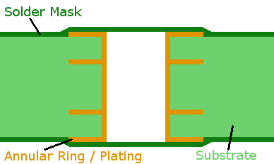

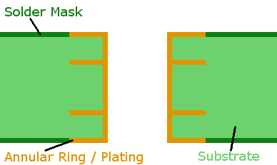


why is via tenting required on a pcb. 28 01 2014 tenting vias is useful wherever smt pads are placed in close proximity to vias it is particularly useful within bga areas where reworking shorts underneath the component is difficult and time consuming feel free to visit our printed circuit board and pcb via process page for further information or download our ebook on pcb design below.
technical tips for pcbs copper thickness controlled. via tenting plugging and filling there are many reasons a printed circuit board designer might want to have a via tented plugged or filled first let s start with defining these terms since they can be frequently misused and misunderstood via tenting this is the easiest and least costly process actually there is no added cost for this. via tenting vs non via tenting for surface mounted pcbs. tenting vias serve many important purposes and come as standard processes under pcb fabrication you can leave vias exposed or plug them completely using conductive and non conductive materials sometimes the bga design uses via in pad technology with space limitations we can manufacture high quality pcbs with via tenting and via plugs. tenting via the ultimate guide to the importance of pcbs. 28 01 2019 why is pcb via tenting important tenting vias of a printed circuit board is a common practice to protect printed circuit boards it is often preferred over mask plugging or epoxy filling because of cost the most cost effective form of via tenting is lpi or liquid photoimageable solder mask tenting. guide to pcb via tenting mcl. tenting vias plugged vias and via in pad as we all know there is a confusion about tenting vias and plugged vias when placing your pcb order many customers and designers get into trouble in learning which one is better. tenting vias plugged vias and via in pad pcbgogo. via tenting plugging and filling there are many reasons a printed circuit board designer might want to have a via tented plugged or filled first let s start with defining these terms since they can be frequently misused and misunderstood.
via tenting plugging and filling pcb prime. 5 1 via tenting via tenting is the procedure to make tented vias they have a non conductive solder mask covering them in this case you should not worry about filling the pcb vias this procedure can also develop a small space with air confined in the via. via tenting plugging and filling wellpcb. pcb vias aid in making more compressed designs by routing traces via the pcb rather than on the surface it supplies a conductive way for an electrical signal to go from one circuit layer to one more. pcb via ultimate guide on all the things you need to know. the main purpose of a pcb via is to provide a conductive path for passing electrical signals from one circuit layer to another by means of a plated hole wall however while all vias perform similar functions each type needs to be accurately documented for reliable assembly and performance. pcb vias everything you need to know.
pcb adalah,pcb ac,pcb ac daikin,pcb amplifier,pcb ac lg,pcb artinya,pcb assembly,pcb ac sharp,pcb ac panasonic,pcb airport,via agent,via adalah,via apk,via avrilia,via appia,via amsterdam,via app,via agent indonesia,via admin,via audio driver,tenting adalah,tenting a house,tenting a turkey,tenting a house for termites,tenting at duke,tenting a roast,tenting a house cost,tenting aluminum foil,tenting a steak,renting a car

0 Response to "Pcb Via Tenting"
Posting Komentar