![LED PCB board design Guidelines [Part 1] | 4MCPCB](https://lh3.googleusercontent.com/blogger_img_proxy/AEn0k_uElT5JoO2JvHpP578E7GEPSHKuN44K2Kyv-tnQ6q6XFkp94pXNQLwv5ZEffT1sH6Bz4WycxC4FpXgxTVL5BcI5swAkG61zkYJ17Ui6xIx42XUQnwQY5HsrYduYKbdzSVCLfPW3arJBtGIm7dWf9ZOJ8Va_LJ4to9Ctm4RO1y9fA2uXYvpmN-g=s0-d)


pcb via size guidelines for manufacturing vse. 30 07 2019 if vias aren t planned out correctly they can cause problems during the manufacturing of your board let s take a look then at some of the common problems that can happen during pcb manufacturing with vias and how you and your cm can avoid these problems by following good pcb via size guidelines.
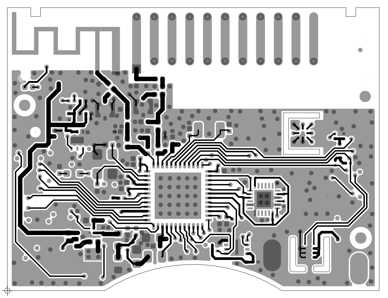
pcb design layout guidelines hints tips electronics. eurocircuits pcb design guidelines have been created to help design engineers create pcb layouts that are right first time for manufacture. a complete guide to vias in pcb design electronics post. 03 12 2018 you gotta love those mutually exclusive requirements rather than just telling you no never here are a few guidelines on how to do it properly pcb assemblers don t like it but with some designs if done properly there can be a number of compelling reasons for putting vias directly in the smt pads for bga and qfn packaged components. pcb design guidelines eurocircuits eurocircuits pcb. via holes all via holes are plated through holes and are defined by default as hole that is 0 45mm 18mil in diameter we allow for via holes to have a maximum negative tolerance of 0 30mm 12mil and may be reduced to accommodate a larger annular ring if required. via in pad guidelines for printed circuit boards pcbs. pcb via size are the key features in the multilayer pcb via construction consists of three major components a metal plated hole solder pads on either side and insulation and clearance along the entire via content 1 pcb via types 2 standard pcb via size 3 pcb aspect ratio 1 pcb via types pcb vias are classified into three different types. pcb design guidelines drilled holes eurocircuits. 03 09 2017 design guidelines for vias in pcb minimum size of the via that can be drilled can be checked with the fabrication house that you are aiming at for your design then capacitance has be to.
pcb via size complete information it s here ourpcb. it gives you a good size to shoot for here is what completed vias look like on the board it is important to note that small vias will cost you quite a bit more than regular size ones generally i don t recommend going below an 8 mil drill a microvia is a via that is less than 6. design guidelines for vias in pcb. the pcb fab throws the pcb in the through hole plating bath until an appropriate thickness of metal grows in every hole i generally pick a via size that i know is greater than or equal to the preferred minimum hole size capability at many different pcb fab houses so i m not locked into a. pcb how to chose via diameter and drill size based on. pcb standard via sizes electrical engineering stack.
pcb adalah,pcb ac,pcb ac daikin,pcb amplifier,pcb ac lg,pcb artinya,pcb assembly,pcb ac sharp,pcb ac panasonic,pcb airport,via adalah,via apk,via avrilia,via appia,via amsterdam,via app,via agent indonesia,via admin,via audio driver,via agent login,size a4,size a5,size a3,size a2,size adidas,size a6,size a5 cm,size a3 cm,size a4 cm,size adidas cm,guidelines adalah,guidelines artinya,guidelines aha,guidelines asthma 2019,guidelines advertising,guidelines and procedures,guidelines atrial fibrillation,guidelines app,guidelines and procedures for using email,guidelines asthma

0 Response to "Pcb Via Size Guidelines"
Posting Komentar