


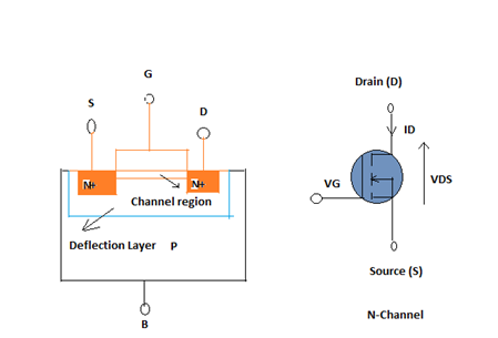


what is a fet explain its working using circuit diagrams. 01 03 2016 did you just copy paste a question from the university s question paper or what p anyway since you asked for it the field effect transistor fet is a transistor that uses an electric field to control the shape and hence the electrical conduct.
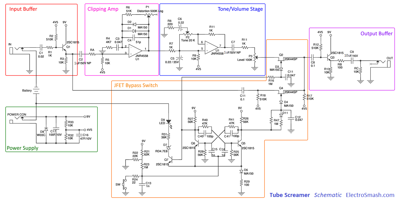
jfet junction field effect transistor construction symbol. dumble heaven dumble overdrive specials 60 s ods preamp 60 s ods poweramp 60 s ods output 70 s ods preamp 70 s ods overdrive 70 s ods poweramp 70 s ods output 97 ods full schematic 97 dumble ods notes 97 ods notes generic dumble circuits dumble ator ods jfet input 90 s ods block diagram mods for ab763 fenders. dumble heaven amp schematics ods overdrive special steel. 18 04 2017 after watching this video you will be able to 1 describe what is jfet amplifiers 2 draw and explain the block diagram of jfet amplifier 3 draw the circuit symbol of jfet amplifier 4 explain. images of block diagram of jfet. a fet curve tracer is a specialised piece of electronic test equipment used to analyse the characteristic of the fets it displays the so called v i voltage versus current graph on an oscilloscope screen whilst the voltage level at gate terminal contributes different characteristic the curve tracer is specifically designed to plot a. jfet amplifiers electronics engineering by raj kumar. a block diagram of the qs3384 cmos bus switch is shown in figure 1 this 10 bit switch or as a 5 bit 2 to 1 multiplexer a block diagram of the qs3383 cmos bus exchange switch is shown in figure 2 this device consists of two banks of ten an ow n a0 b0 switch block diagram mapn 00009 01 quality semiconductor inc 1 an 09 table 3 pin. fet curve tracer universiti tunku abdul rahman. jfet characteristics depletion regions an n channel jfet characteristics block representation is shown in some detail in fig 9 6 with a drain source voltage applied as illustrated i d flows in the direction shown producing voltage drops along the channel consider the voltage drops from the source terminal s to points a b and c within the channel.
a simple radio receiver university of cambridge. bipolar junction transistors bjt general configuration and definitions the transistor is the main building block element of electronics it is a semiconductor device and it comes in two general types the bipolar junction transistor bjt and the field effect transistor fet here we will describe the system characteristics of the bjt. simple switch block diagram datasheet applicatoin notes. jfet characteristics drain characteristics transfer. transistors bipolar junction transistors bjt. what is the mosfet basics working principle and applications.
block ads,block adalah,block ads chrome,block app in firewall,block autocad,block artinya,block ads chrome android,block and tackle,block ads youtube,block all incoming calls android,diagram alir,diagram alir penelitian,diagram adalah,diagram activity,diagram alir adalah,diagram alir proses,diagram aktivitas,diagram alir proses produksi,diagram analisis swot,diagram alir data,of adalah,of artinya,of all time,of adalah penyakit,of all meaning,of approximately,of a kind,of age meaning,of a lifetime,of all the cereals rice is the one,jfet adalah,jfet analog switch,jfet amplifier,jfet and mosfet,jfet and mosfet pdf,jfet and mosfet difference,jfet and bjt,jfet ac analysis,jfet and mosfet comparison,jfet and fet

0 Response to "Block Diagram Of Jfet"
Posting Komentar