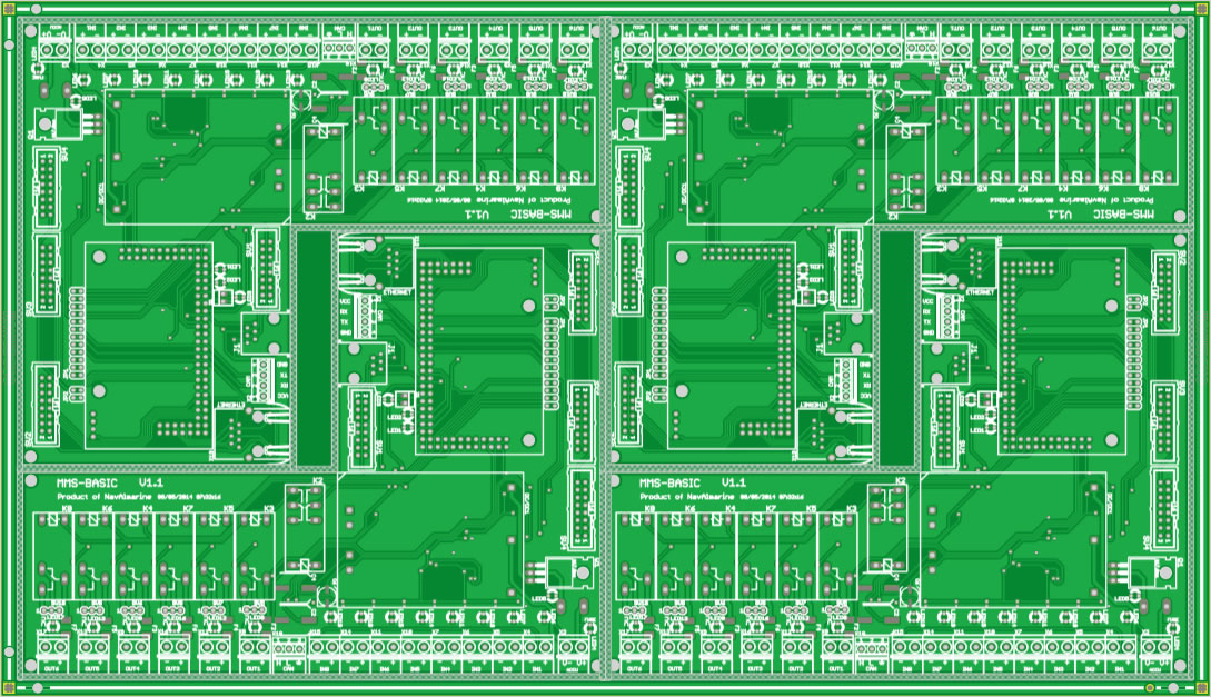


tooling holes pcb. the general term for holes placed on a pcb or a panel of pcbs for registration and hold down purposes during the manufacturing process also known as fabrication hole pilot hole or manufacturing hole the recommended tooling holes diameter is 2mm 78 74mil.
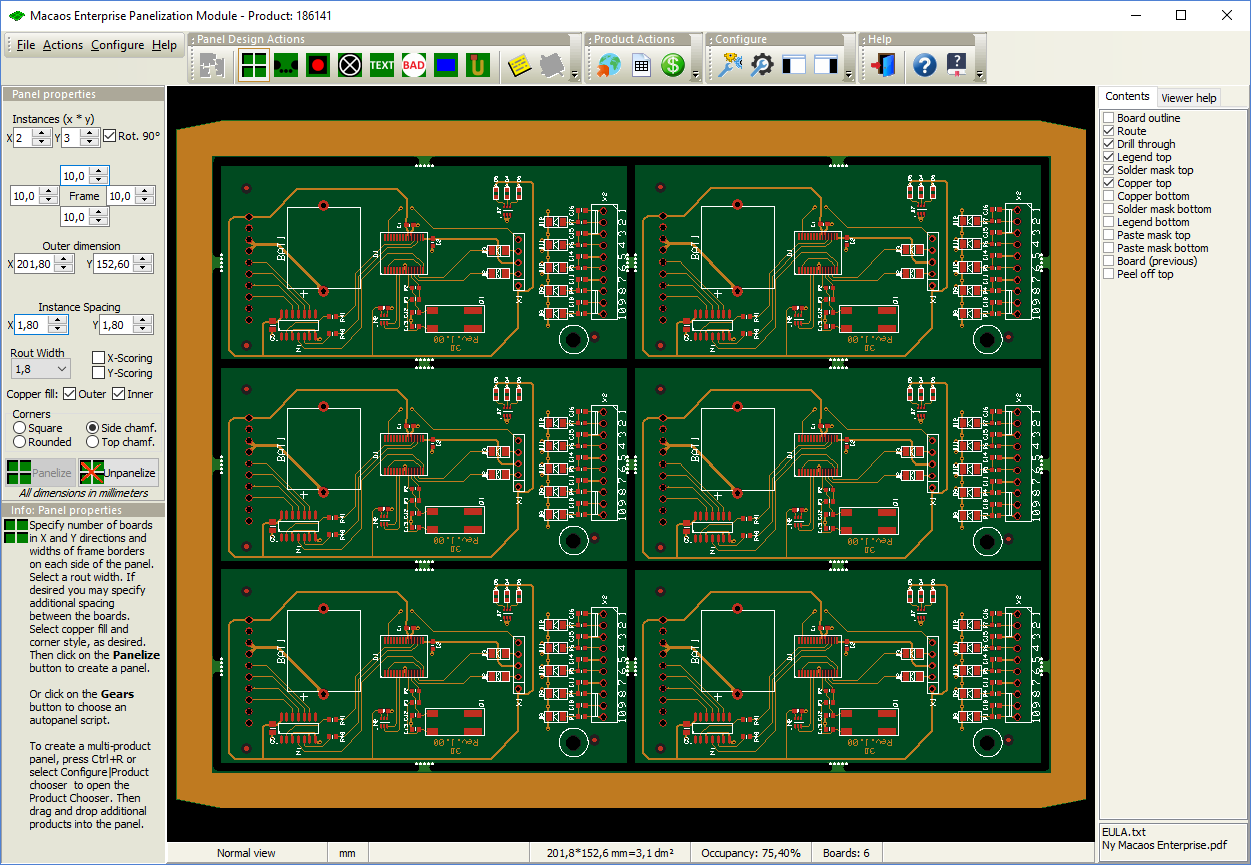
panel requirements for printed circuit board assembly. panel requirements for pcb assembly fiducial marks and mounting holes in panel 1 fiducial marks for each panel we require at least 3 fiducial marks those marks should be placed in the middle of the tooling strips with the diameter at 1 0mm. merifix pcb design guide introduction. merifix pcb design guide page 1 merifix electronics www merifix com tooling holes tooling holes are added to boards for a variety of for some of these purposes tooling holes can be placed in the overall panel but for activities that occur after de panelling or for boards that are. pcb panel parameters dzone iot. find out more about pcb panel parameters such as arrays pcb tooling rail fiducials tooling holes scoring and more. connectors tooling holes and fiducial markers for. the standard practice would be to add three fiducials to the panel in three of the four corners on both sides of the pcb so the machine can determine if the pcb has been loaded incorrectly adding tooling holes within the handling edges depending if required by the machines that are intended to be used. pcb panel design surface mount process. 19 07 2011 if you have pcb s that are 2 dense and or small for tooling holes you can have an ate jig made for the whole panel and have the tooling holes on the panel border i have done this in the past where ever you put the tooling holes you will have to provide some information for the jig to be made.
problem with tooling holes in a pcb. a printed circuit board pcb the outer tooling strip often includes tooling holes a set of panel fiducials a test coupon and may include hatched copper pour or similar patterns for even copper distribution over the whole panel in order to avoid bending the assemblers often mount components on panels rather than single pcbs because this. printed circuit board wikipedia. other mechanical feature must come within 0 200 5 00 of the edge of the pcb in this case 0 120 3 00 tooling holes must be added within the pcb outline in two opposite corners to allow for screen printing alignment there must also be a component free circular area around the tooling holes of 0 236 6 00 diameter centred on the tooling hole. technical note tn004 pcb panel design guidelines. 15 12 2015 tooling holes to facilitate bed of nails testing provide tooling holes near any three corners of the board arrays on the breakaway processing edges tooling holes. pcb designers need to know these panelization guidelines.
pcb adalah,pcb ac,pcb ac daikin,pcb amplifier,pcb ac lg,pcb artinya,pcb assembly,pcb ac sharp,pcb ac panasonic,pcb airport,panel adalah,panel ats,panel akustik,panel arsitektur,panel ats amf,panel acp,panel aluminium,panel artinya,panel asri perkasa,panel anggota himpenindo,tooling adalah,tooling artinya,tooling around,tooling api salesforce,tooling around town,tooling amortization,tooling and manufacturing association,tooling agreement,tooling and engineering,tooling api objects,holes author,holes actors,holes audiobook,holes anatomy and physiology,holes anatomy and physiology 15th edition,holes activities,holes amazon prime,holes and electrons,holes anatomy and physiology 14th edition,holes amazon

0 Response to "Pcb Panel Tooling Holes"
Posting Komentar