

pcb design beginnerpcb design beginner emtech. join our 4 week pcb design course to know complete pcb manufacturing process and become capable of designing your own project pcb s that are upto industrial grade target keyword pcb design course pcb manufacturing process 4 week training pcb design course in delhi electronics manufacturing electronics product design job assistant courses.
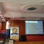
a report on two days workshop on pcb and circuit. a report on two days workshop on pcb and circuit designing 16 organized by s o s in electronics photonics in association with robo tech india pvt lmtd. department of electronics computer engineering a. department of electronics computer engineering a report on pcb design workshop the dept of ecm under the guidance of embedded systems research group organized a two day work shop on pcb design on january 24th and 25th total 197 students were registered for the workshop from ecm ece and eee departments. report on two day workshop on pcb design and. report on two day workshop on pcb design and fabrication 31 08 2017 01 09 2017 on behalf of department of ece gnit in association with iete students forum and ece department association we have organized a two day workshop on pcb design and fabrication on 31 08 2017 and 01 09 2017 in collaboration with pgp electronics pvt ltd. report on pcb design and fabrication workshop. the workshop started with an introductory and interactive talk on pcb design the resource person for the workshop was mr toshal madkaikar alumni of don bosco college of engineering the circuit implemented on the pcb was an astable multivibrator. p cad 2002 pcb user s guide final. p cad pcb user s guide i table of contents chapter 1 introduction to p cad pcb p cad pcb features 1.
engineering training report. learning different programs such as dip trace for printed circuit board pcb design c language for pic programming and proteus simulator studying the common types of serial interfaces rs232 rs422 and rs485 and how to communicate with a computer using them designing pulse width modulation pwm circuits. report on pcb designing and fabrication workshop. report on pcb designing and fabrication workshop organised by electrical engineering department report on pcb designing and fabrication workshop organised by electrical engineering department electrical pcb workshop download. advanced pcb layout course fedevel. this course covers all the important subjects you need to know for advanced pcb layout placement how to place cpu memories power supplies connectors protection etc basic rules basic stackup initial rules and stackup settings to start your layout report abuse. top 10 pcb routing tips for beginners eagle blog. if this is your first time doing a pcb layout then seeing a chaotic looking ratsnest might be a little intimidating use these top 10 pcb routing tips and also our top 10 component placement tips to make your first pcb layout a success tip 1 don t rely on your autorouter.
pcb adalah,pcb ac,pcb ac daikin,pcb amplifier,pcb ac lg,pcb artinya,pcb assembly,pcb ac sharp,pcb ac panasonic,pcb airport,designing and managing integrated marketing channels,designing a logo,designing artinya,designing and managing services,designing app,designing and managing integrated marketing communications,designing and managing the supply chain,designing a website,designing api,designing a poster,workshop adalah,workshop artinya,workshop akuntansi,workshop andika sutoro putra,workshop arsitektur,workshop adalah pelatihan,workshop anak,workshop alat berat,workshop agenda,workshop adalah wikipedia,report adalah,report artinya,report akun ig,report analysis,report akun youtube,report akun fb,report account instagram,report and block whatsapp,report and block whatsapp artinya,report akun instagram penipu

0 Response to "Pcb Designing Workshop Report"
Posting Komentar