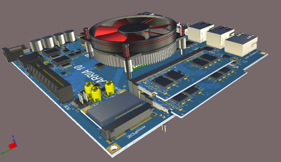


printed circuit board wikipedia. a printed circuit board pcb mechanically supports and electrically connects electrical or electronic components using conductive tracks pads and other features etched from one or more sheet layers of copper laminated onto and or between sheet layers of a non conductive substrate.
pcb software wikipedia. components are generally soldered onto the pcb to both electrically connect and mechanically fasten them to it printed circuit boards are used in all but the simplest electronic products they are also used in some electrical products such as passive switch boxes. eagle program wikipedia. components are generally soldered onto the pcb to both electrically connect and mechanically fasten them to it printed circuit boards are used in all but the simplest electronic products they are also used in some electrical products such as passive switch boxes alternatives to pcbs include wire wrap and point to point construction both once popular but now rarely used pcbs require additional design effort to lay out the circuit but manufacturing and assembly can be automated specialized cad software is available to do much of the work of layout mass producing circuits with pcbs is cheaper and faster than with other wiring methods as components are mounted and wired in one operation large numbers of pcbs can be fabricated at the same time and the layout only has to be done once pcbs can also be made manually in small quantities with reduced benefits pcbs can be single sided one copper layer double sided two copper layers on both sides of one substrate layer or multi layer outer and inner layers of copper alternating with layers of substrate multi layer pcbs allow for much higher component density because circuit traces on the inner layers would otherwise take up surface space between components the rise in popularity of multilayer pcbs with more than two and especially with more than four copper planes was concurrent with the adoption of surface mount technology however multilayer pcbs make repair analysis and field modification of circuits much more difficult and usually impractical read more on wikipedia. altium designer wikipedia. pcb was first written by thomas nau for an atari st in 1990 and ported to unix and x11 in 1994 initially pcb was not intended to be a professional layout system but as a tool for individuals to do small scale development of hardware the second release 1 2 introduced user menus this made pcb easier to use and increased its popularity harry eaton took over pcb development beginning with release 1 5 although he contributed some code from release 1 4 3. proteus design suite wikipedia. eagle is a scriptable electronic design automation eda application with schematic capture printed circuit board pcb layout auto router and computer aided manufacturing cam features eagle stands for easily applicable graphical layout editor german einfach anzuwendender grafischer layout editor and is developed by cadsoft computer gmbh the company was acquired by. which pcb design software is most used quora. protel dxp was issued in 2003 protel 2004 in 2004 altium designer 6 0 in 2005 altium designer version 6 8 from 2007 was the first to offer 3d visualization and clearance checking of pcbs directly within the pcb editor in may 2014 altium relocated their corporate headquarters to san diego california features.
top 9 best pcb design software of 2019 latest with seeed. all pcb design products include an autorouter and basic mixed mode spice simulation capabilities schematic capture schematic capture in the proteus design suite is used for both the simulation of designs and as the design phase of a pcb layout project it is therefore a core component and is included with all product configurations. altium designer ivc wiki. 19 09 2018 most popular pcb design softwares are they all can do high speed pcb designs 1 altium 2 orcad 3 kicad 4 eagle 5 allegro 6 pads 7 xpedition you can read more. 10 free pcb design software electroschematics com. printed circuit board top 9 best pcb design software of 2019 by liyan gong 3 years ago there are many circuit design softwares available to satisfy diversified layout requirement including free pcb design software online free pcb design softwares and industrial pcb softwares this is the pcb design software list and brief introduction. papan sirkuit cetak wikipedia bahasa indonesia. multiple board design to keep multiple pcb boards design updated each separate board has to be kept in individual pcbprjct files all the schematics are then added to a master project with only scdoc files no pcbdoc files this keeps all the net and rules the same for the schematics but the pcb layout nested see this article for details.
pcb adalah,pcb ac,pcb ac daikin,pcb amplifier,pcb ac lg,pcb artinya,pcb assembly,pcb ac sharp,pcb ac panasonic,pcb airport,designing and managing integrated marketing channels,designing a logo,designing artinya,designing and managing services,designing app,designing and managing integrated marketing communications,designing and managing the supply chain,designing a website,designing api,designing a poster,wiki adalah,wiki addict,wiki azur lane,wikiapbn,wiki asia,wiki aqw,wiki a bizarre day,wiki ad astra,wiki alphabet robot,wiki arknights

0 Response to "Pcb Designing Wiki"
Posting Komentar