
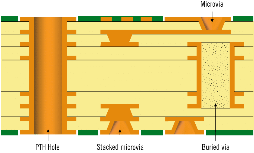

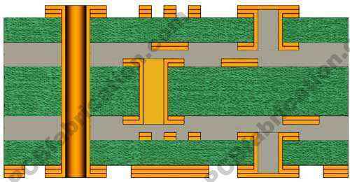


blind vias buried vias multi circuit boards. blind buried vias due to the increasing complexity of design structures blind vias and buried vias are increasingly used in high density circuit boards a blind via connects exactly one outer layer with one or more inner layers a buried via is a via between at least two inner layers which is not visible from the outer layers this technology allows more functionality in less board space.
via electronics wikipedia. in printed circuit board design a via consists of two pads in corresponding positions on different layers of the board that are electrically connected by a hole through the board the hole is made conductive by electroplating or is lined with a tube or a rivet high density multilayer pcbs may have microvias blind vias are exposed only on one side of the board while buried vias connect internal layers without being exposed on either surface thermal vias carry heat away from power devices and are typically used in. blind and buried pcb vias pcbcart. pcbcart specializes in a variety of vias for pcb fabrication and assembly including blind vias buried vias through hole vias stacked vias and microvias get started on your pcb assembly project by request a free pcba quote. blind and buried vias eurocircuits eurocircuits blind. blind and buried vias blind and buried vias are used to connect between layers of a pcb where space is at a premium a blind via connects an outer layer to one or more inner layers but does not go through the entire board a buried via connects two or more inner layers but does not go through to an outer layer but not all combinations are possible. reduce your pcb costs with blind vias buried vias and. 18 01 2020 buried via buried vias provide an even more superior level of space saving on the surface and consequently compacting the overall pcb even more since buried vias are only placed between internal layers they allow more space for traces and pads on both outer surfaces this reduces the overall pcb cost by efficient use of space. blind buried vias pcb prototype the easy way pcbway. blind vias and buried vias blind and buried vias are only available on boards with at least four layers unlike regular vias on a two layer board which connect the two surface layers buried and blind vias connect the inner layers with either other adjacent inner layers or adjacent surface layers.
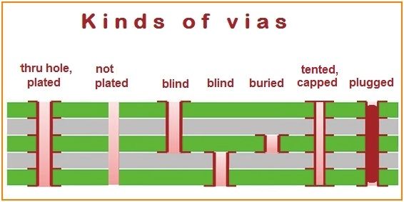
pcb 101 what are blind and buried vias. 31 05 2019 vias are barrel shaped vertical conductive holes that make connections between multiple layers of a pcb the ipc defines eight different types of vias but we re going to talk about blind and buried vias the two you re most likely to work with.
pcb adalah,pcb ac,pcb ac daikin,pcb amplifier,pcb ac lg,pcb artinya,pcb assembly,pcb ac sharp,pcb ac panasonic,pcb airport,buried alive,buried alive lyrics,buried alive chord,buried alive tab,buried alive movie,buried alive avenged sevenfold,buried alive pokemon,buried artinya,buried adalah,buried alive intro tab,via agent,via adalah,via apk,via avrilia,via appia,via amsterdam,via app,via agent indonesia,via admin,via audio driver

0 Response to "Pcb Buried Via"
Posting Komentar