
.JPG)

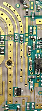


printed circuit board wikipedia. a printed circuit board pcb mechanically supports and electrically connects electrical or electronic components using conductive tracks pads and other features etched from one or more sheet layers of copper laminated onto and or between sheet layers of a non conductive substrate.
what is printed circuit board pcb definition from. components are generally soldered onto the pcb to both electrically connect and mechanically fasten them to it printed circuit boards are used in all but the simplest electronic products they are also used in some electrical products such as passive switch boxes. pcb basics learn sparkfun com. components are generally soldered onto the pcb to both electrically connect and mechanically fasten them to it printed circuit boards are used in all but the simplest electronic products they are also used in some electrical products such as passive switch boxes alternatives to pcbs include wire wrap and point to point construction both once popular but now rarely used pcbs require additional design effort to lay out the circuit but manufacturing and assembly can be automated specialized cad software is available to do much of the work of layout mass producing circuits with pcbs is cheaper and faster than with other wiring methods as components are mounted and wired in one operation large numbers of pcbs can be fabricated at the same time and the layout only has to be done once pcbs can also be made manually in small quantities with reduced benefits pcbs can be single sided one copper layer double sided two copper layers on both sides of one substrate layer or multi layer outer and inner layers of copper alternating with layers of substrate multi layer pcbs allow for much higher component density because circuit traces on the inner layers would otherwise take up surface space between components the rise in popularity of multilayer pcbs with more than two and especially with more than four copper planes was concurrent with the adoption of surface mount technology however multilayer pcbs make repair analysis and field modification of circuits much more difficult and usually impractical read more on wikipedia. home printed circuits llc. printed circuit board pcb a printed circuit board pcb is the board base for physically supporting and wiring the surface mounted and socketed components in most electronics. pcb design how to create a printed circuit board. printed circuit board is the most common name but may also be called printed wiring boards or printed wiring cards before the advent of the pcb circuits were constructed through a laborious process of point to point wiring this led to frequent failures at wire junctions and short circuits when wire insulation began to age and crack. printed circuit boards manufacturer high technology pcb. printed circuit boards pcbs connect electrical components together using discrete wiring resulting in a complete and functional unit pcbs can be as simple as one or two layers of copper circuits but are far more likely to have many layers of circuitry the layers are necessary for the designer to route all of the circuits between.
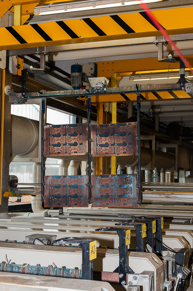
how to make a printed circuit board pcb at home youtube. pcb design how to create a printed circuit board to create a printed circuit board pcb you need to draw holes pads and wires for your circuit this skill is called pcb design and is highly useful when you re done send the design to a manufacturer or you etch it yourself. pcb design software printed circuit boards autodesk. delivering quality pcbs since 1952 for more than 65 years epec has continued its tradition of perfection in engineering and manufacturing printed circuit boards our reliability and financial stability has made us an industry leading provider of time critical high performance pcb solutions. printed circuit board milling wikipedia. 26 09 2015 how to make a printed circuit board pcb at home by watching this simple tutorial you will be able to make your own pcb at home category howto style show more show less. how printed circuit board is made material manufacture. printed circuit board pcb design brings your electronic circuits to life in the physical form using layout software the pcb design process combines component placement and routing to define electrical connectivity on a manufactured circuit board. related searches for printed circuit pcb. printed circuit board milling also isolation milling is the process of removing areas of copper from a sheet of printed circuit board material to recreate the pads signal traces and structures according to patterns from a digital circuit board plan known as a layout file.
printed advertisement,print a3,print a2,print a3 terdekat,print area excel,print and print,print ad,print amplop,print array php,print art paper,circuit adalah,circuit analysis,cricut australia,cricut alternative,circuit app,circuit arcade bar,cricut air 2,circuit apartments,circuit analyzer,circuit abbreviation,pcb adalah,pcb ac,pcb ac daikin,pcb amplifier,pcb ac lg,pcb artinya,pcb assembly,pcb ac sharp,pcb ac panasonic,pcb airport

0 Response to "Printed Circuit Pcb"
Posting Komentar