


designing pcbs smd footprints learn sparkfun com. as new ics come out the pcb layout softwares of the world will not have that specific part within their component libraries for example eagle may have a given footprint soic 8 or qfn 24 but i wouldn t trust it i have lost so much money on pcbs that had the wrong footprint that i don t use the built in libraries eagle or other.
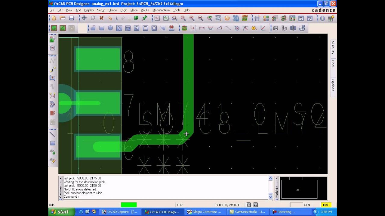
what does a footprint mean in pcb design quora. 08 10 2017 a footprint also called a land pattern is used during board layout and is where an electronic component gets soldered onto the pcb it consists of several layers of information including the copper lands silkscreen the text and shapes you. footprint electronics wikipedia. a footprint or land pattern is the arrangement of pads in surface mount technology or through holes in through hole technology used to physically attach and electrically connect a component to a printed circuit board the land pattern on a circuit board matches the arrangement of leads on a component component manufacturers often produce multiple pin compatible product variants to allow. how to design a pcb layout circuit basics. making sure your printed circuit board does become a printed circuit is a priority after all have a design tool that can manage solder electronic components schematic design and component placement without drowning you in pcb design tools that are unintuitive to use on a circuit board or would require a pcb design tutorial. pcb designing tutorial altium designer for your maker needs. scalable pcb design invest for the future with a pcb design solution that can provide the capabilities you need today with the ability to seamlessly grow as your designs requirements increase virtual prototyping analyze your designs over millions of potential conditions before you ever build a prototype and achieve first pass success. orcad pcb editor tutorial 01 assigning footprints to your. easyeda is a free and easy to use circuit design circuit simulator and pcb design that runs in your web browser.
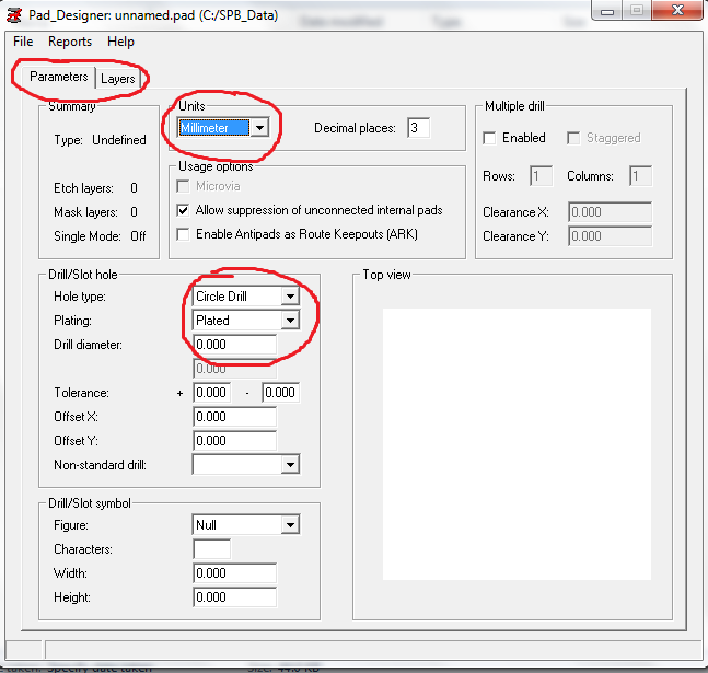
easyeda online pcb design circuit simulator. 29 05 2018 the four w s of footprint pad layout guidelines your pcb layout may contain several different types of pads generically a pad is an electrical connection point that may join two component pins a component pin and a trace a trace and a via or even a trace with an external or off board device. best footprint pad layout guidelines for your pcb tempo. 11 12 2019 the ipc footprints batch generator has options to either create all the footprints in the open pcb footprint library or generate a single library based on either an input file or footprint name creating a component using the footprint wizard the pcb library editor includes a footprint wizard. creating the pcb footprint altium designer 20 0 user. snapeda was a lifesaver in our most recent board design project we were working on a very tight deadline and didn t have footprints for several of the components that we needed to use snapeda saved us many hours compared with creating footprints by hand. snapeda free pcb footprints and schematic symbols.
designing and managing integrated marketing channels,designing a logo,designing artinya,designing and managing services,designing app,designing and managing integrated marketing communications,designing and managing the supply chain,designing a website,designing api,designing a poster,pcb adalah,pcb ac,pcb ac daikin,pcb amplifier,pcb ac lg,pcb artinya,pcb assembly,pcb ac sharp,pcb ac panasonic,pcb airport,footprint adalah,footprint artinya,footprint art,footprint and handprint game,footprint analysis,footprint and handprint,footprint area,footprint app,footprint architects,footprint animals

0 Response to "Designing Pcb Footprint"
Posting Komentar