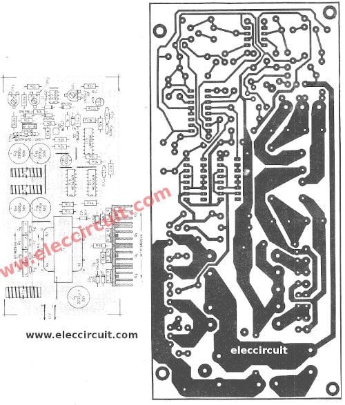


ac to dc converter circuit diagram. 26 06 2018 step 2 transferring the design data from the schematic to pcb layout now we are ready to convert a schematic to a pcb layout but first we need a pcb to transfer too right click on the project and select add new to project pcb as shown in the picture below this will create a pcb object in your project tree.
how to create a pcb layout from a schematic in altium. layout design figure 1 4 switch synchronous buck boost converter schematic design of a new 3 bit flash analog to digital converter adc aided design software for the schematics and printed circuit board pcb layout respectively pcb design software schematic capture software spice simulation and automatic 3d model generation the pcb. how to design a pcb layout circuit basics. 18 09 2019 here are some pcb layout tips that can help you to create a good and reliable dc dc buck converter design on your next printed circuit board layout a good layout for a dc dc buck converter design on your printed circuit board is essential to its successful operation here are some layout tips that can help. schematic to pcb converter wordpress com. 18 05 2016 in this video i will create a pcb layout for my attiny boost converter with the help of the free software easyeda easyeda pcb design and order from free online schematic pcb design. layout tips for your dc dc buck converter design. learn best layout practices for your dc dc buck converter circuits in implementing dc dc buck converters circuit layout is just as important as design a great design can be severely degraded by bad layout this article will go over some best layout practices goals of good circuit layout here are some goals of good layout to keep in mind. easyeda free schematic pcb design simulation. 16 04 2008 you can then create a pcb file from this netlist generally the pcb file will initially show you all of your parts with a bunch of lines between them called a ratsnest this is how the pcb editor shows you what connects to what according to your schematic file to confirm if your pcb layout is correct use drc design rules check.
tips and techniques for dc dc buck converter pcb layout. 28 08 2018 technical article guide to pcb design from pcb schematic to board layout august 28 2018 by robert keim in this article you will learn the basics of how to plan a schematic for a custom pcb and lay out your pcb prototype design. schematic to pcb layout all about circuits. circuit schematic design everything starts with an idea then comes circuit schematic diagram and finally comes pcb design schematic diagram design is the basis of pcb design correlated with effect of pcb design so that if something goes wrong in schematic diagram. guide to pcb design from pcb schematic to board layout. a guideline from schematic to pcb design based on altium.
pcb adalah,pcb ac,pcb ac daikin,pcb amplifier,pcb ac lg,pcb artinya,pcb assembly,pcb ac sharp,pcb ac panasonic,pcb airport,layout adalah,layout android,layout apotek,layout artinya,layout apk,layout autocad,layout apartemen,layout apartemen studio,layout app,layout amplop,to all the boys,to all the boys 2,to all the boys i loved before book,to all the boys 3,to aipki,to aru kagaku no railgun,to aru majutsu no index,to artinya,to and fro,to all boys i loved before,schematic arduino uno,schematic adalah,schematic arduino nano,schematic advan e1c 3g,schematic acer e5-411,schematic arduino uno r3,schematic asus x014d,schematic asus z00ad,schematic acer z1401,schematic asus x453ma rev 2.0,converter avi to mp4,converter adalah,converter ac to dc,converter ac ke dc,converter adaptor,converter ata to sata,converter aux to usb,converter audio to mp3,converter av to hdmi,converter apk

0 Response to "Pcb Layout To Schematic Converter"
Posting Komentar